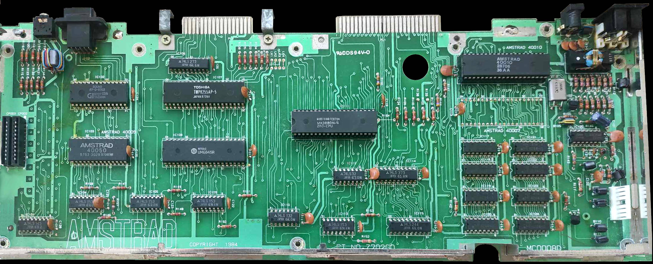
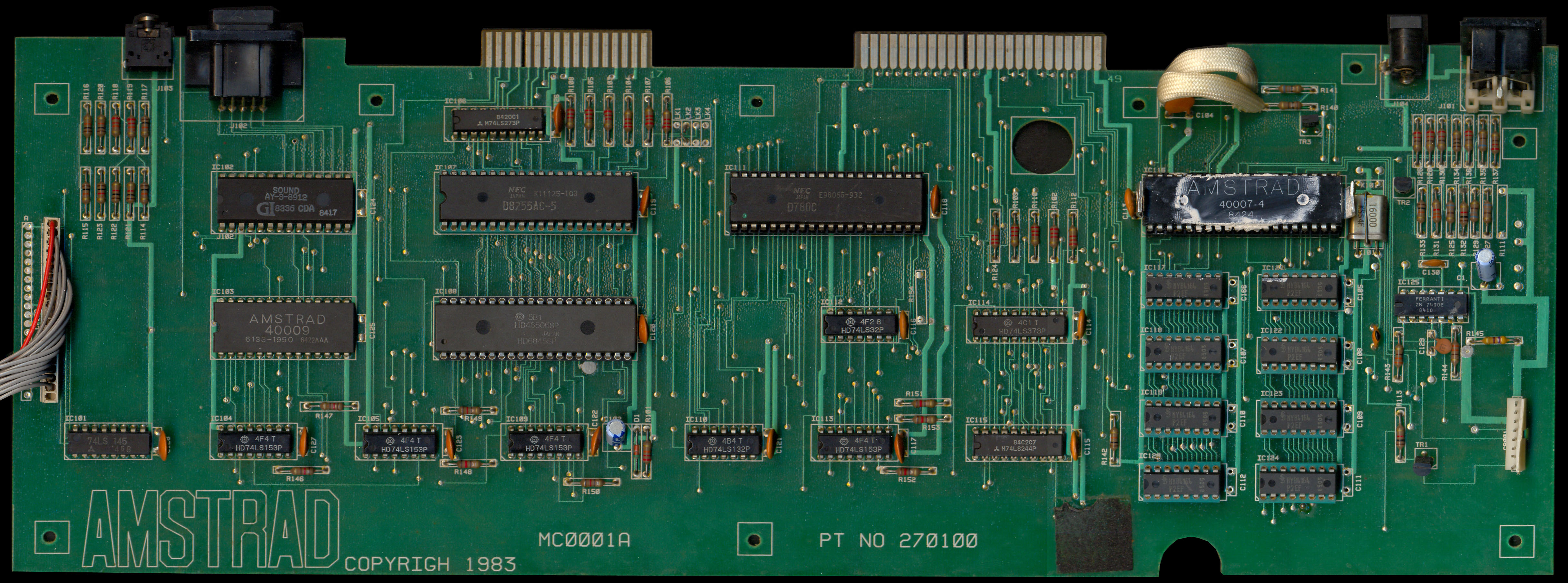
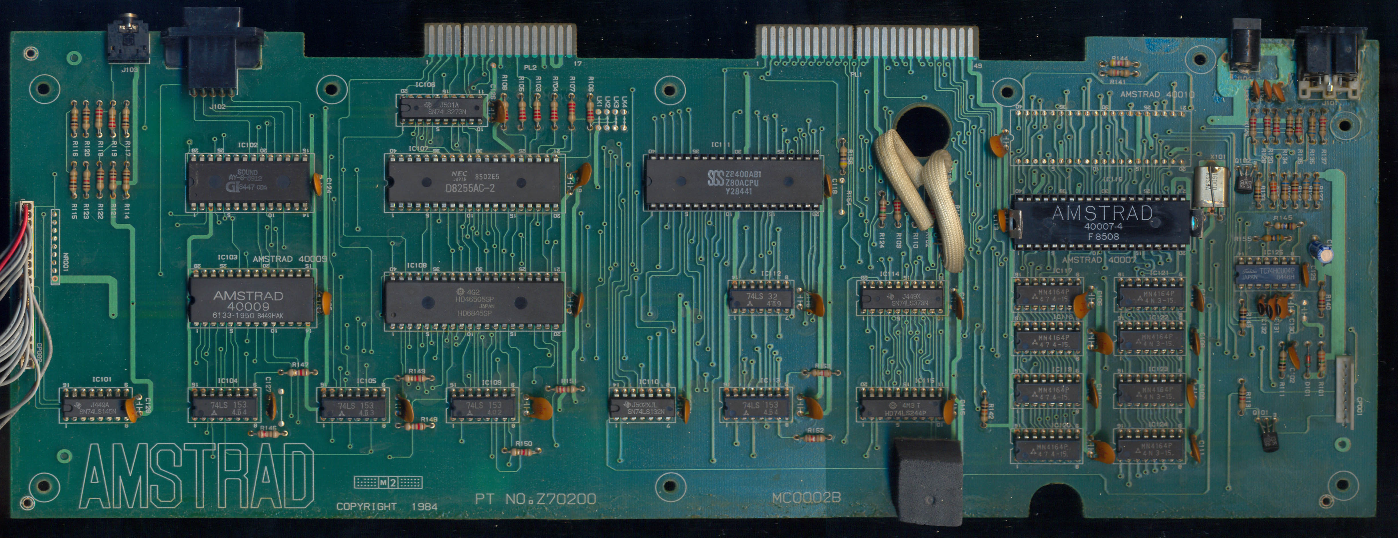
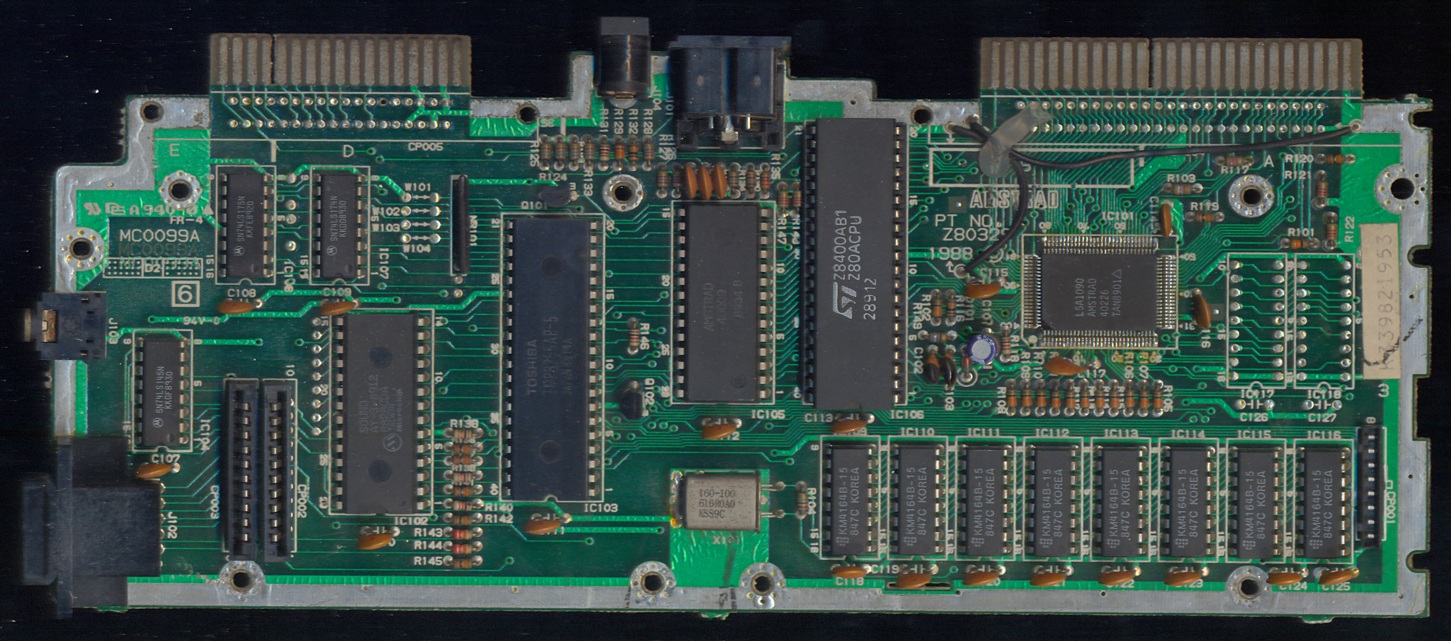
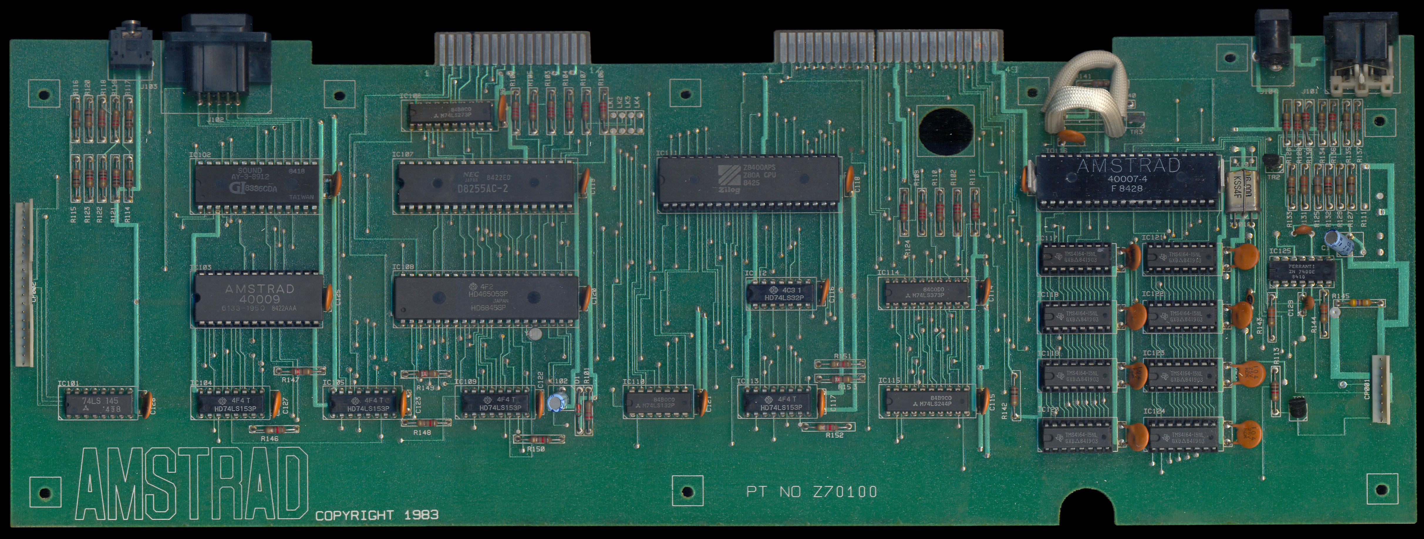
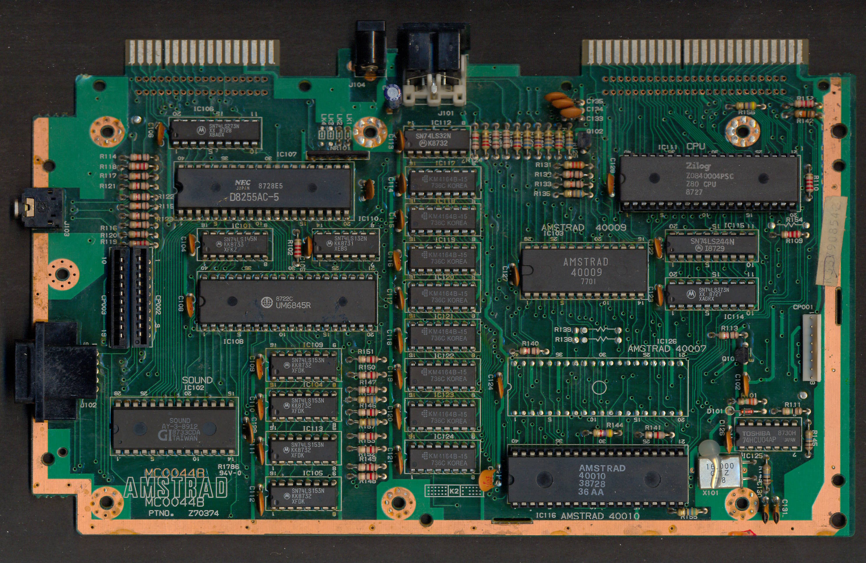
The Z80 is an 8-bit microprocessor designed by Zilog founder and CEO Federico Faggin, first released in July 1976. It is the CPU used in the Amstrad CPC / Plus / PCW computers.
The Z80/Z80A was a very popular microprocessor, used in a wide range of applications, from early gaming consoles like the ColecoVision or the Sega Master System to personal computers like the ZX Spectrum and the MSX.
It was even used in the Sega MegaDrive as the sound CPU and in the Commodore C128 as a secondary processor in order to achieve CP/M compatibility.
Also, an in-between the Intel 8080 and the Z80 powers the original Nintendo Gameboy.
Description
The Z80 microprocessor is an 8-bit CPU with a 4-bit ALU and a 16-bit address bus capable of direct access to 64KB of memory space. The Z80 is a little-endian CPU, meaning it stores 16-bit values with the least significant byte first, followed by the most significant byte. It has a language of 252 root instructions and with the reserved 4 bytes as prefixes, access to an additional 308 instructions.
The Zilog Z80 is an upgraded version of the Intel 8080 and is fully compatible with it at the software level. It contains the seventy-eight 8080 opcodes as a subset to its language. The Z80 adds more registers, better instructions, faster performance, and improved interrupt handling, making it more powerful and efficient than the 8080.
While not in the same league as the Intel 80x86 or the Motorola 68000 series, the Z80 is extremely useful for low cost control applications. One of the more useful features of the Z80 is the built-in refresh circuitry for ease of design with DRAMs.
The Z80 has about 8500 transistors. It comes in a 40-pin DIP package. It has been manufactured in A, B, and C models, differing only in maximum clock speed. It also has been manufactured as a stand-alone microcontroller with various configurations of on-chip RAM and EPROM.
Part numbers used in the Amstrad CPC during its lifetime
The Z80 CPU has been manufactured by others, and various Z80s have been used in the construction of the CPC during its lifetime:
All the Z80 CPUs that have been used on CPC and Plus machines are NMOS. Source
Zilog ended the production of the Z80 in April 2024. The chip is still available in ample quantities through NOS chip suppliers.
Modern incarnations
Apart from surplus/new Z80-clones that are quite easy to find, many emulations depend on software implementations of the Z80:
The T80 is a VHDL implementation of the Z80 and Z80A, finished in 2002 on OpenCores
arnold uses InkZ80, written in C++ (apart from the author-designed C simulation)
On OpenCores, there is also a Verilog implementation of the Z80.
Zilog itself offers the eZ80 processor, a new, 50MHz design. Kits now have reached a less-than-prohibitive price range and may be available without a business.
Registers
Register
Size
Description
Notes
B, C, D, E, H, L
8-bit
General-purpose registers
Can form 16-bit pairs: BC, DE, HL
A (Accumulator)
8-bit
Main register for arithmetic, logic, and data transfer
Most used register
F (Flags)
8-bit
bit7 - SF - Sign Flag
bit6 - ZF - Zero Flag
bit5 - F5 - Undocumented by Zilog
bit4 - HF - Half Carry Flag
bit3 - F3 - Undocumented by Zilog
bit2 - PF - Parity Flag (also sometimes used for Overflow)
bit1 - NF - Negation Flag (last ALU op was subtract or compare)
bit0 - CF - Carry Flag
Flags (including F5 and F3) are affected by most operations.
HF and NF are used in the DAA algorithm.
AF', BC', DE', HL'
16-bit
Alternate register set
Swappable with primary registers for fast context switching
SP (Stack Pointer)
16-bit
Points to top of the stack
Used for subroutine calls and interrupt handling
PC (Program Counter)
16-bit
Points to the next instruction
Automatically increments as instructions execute
IX, IY (Index Registers)
16-bit
Used for indexed addressing
Can be split into IXH/IXL, IYH/IYL for 8-bit access
I (Interrupt Vector)
8-bit
Holds base address for interrupt mode 2
Combined with external data to form an interrupt vector
R (Memory Refresh)
8-bit
Increments after each M1 cycle (instruction or prefix fetch) to refresh DRAM
Only the lower 7 bits are incremented
Internal state
Register
Size
Description
Notes
IM (Interrupt Mode)
2-bit
Specifies the interrupt mode (0, 1, or 2)
Controls how interrupts are handled:
IM 0: External devices provide an opcode to execute (most likely an RST instruction). This mode was originally implemented in the Intel 8080 CPU
IM 1: Fixed vector at 0038h
IM 2: Vector provided by I register and external data
IFF1
1-bit
Main Instruction Fetch Flip-Flop
Set when interrupts are enabled, cleared on disable.
When the CPU accepts a maskable interrupt, both IFF1 and IFF2 are automatically cleared, inhibiting further interrupts.
IFF2
1-bit
Stores the state of IFF1 during Non-Maskable Interrupts (NMI)
When an NMI occurs, the processor clears IFF1 to disable interrupts temporarily.
IFF2 stores the previous state of IFF1 so that after the NMI is handled, IFF1 can be restored to its original state.
WZ
16-bit
Internal temporary register pair. Also known as MEMPTR
Used for memory and address calculations.
Normally, you never see the content of this register. But it leaks through F5 and F3 in the BIT b,(HL) instruction. Source
Q
8-bit
Internal register where it assembles the new content of the F register, before moving it back to F
On Zilog NMOS Z80, when the instruction doesn't compute new flags, this register is cleared instead. But not on NEC NMOS Z80. And CMOS Z80 behave in a different way too.
Normally, you never see the content of this register. But it leaks through F5 and F3 in the SCF/CCF instructions. Source
Emulating Q is not strictly necessary. A 1-bit flag, indicating whether the previous instruction computed flags, is enough to emulate the behaviour of SCF/CCF. Source
Also note that while POP AF and EX AF,AF' modify F, they do not compute new flag values.
IR (Instruction Register)
8-bit
Holds the opcode of the currently executing instruction
Internally used, not accessible by the programmer
EIP (Extended Instruction Prefix)
2-bit
Holds the prefix for extended instructions (CB, ED, or none)
Used for extended instruction sets like bitwise ops
IMP (Indexing Mode Prefix)
2-bit
Specifies the indexing mode (DD for IX+d, FD for IY+d, or none for HL)
Indicates use of index registers (IX or IY) for memory access
8-bit general purpose register (a, b, c, d, e, h, l)
rrr (or sss) = 111, 000, 001, 010, 011, 100, 101
S
Restart address (0x00, 0x08,..., 0x38)
sss = 000, 001,..., 111
Flags
- = no change
+ = change by definition (if noted, by the operation marked with '=> flags', otherwise by the only non-single-bit operation):
* S = sign, bit 7 of the result byte (accumulator or high byte for 16-bit operations)
* Z = zero, set if the result is zero (8 or 16-bit value)
* 5 = undocumented, bit 5 of the result byte
* H = half-carry, the carry (theoretical bit 4) of the low nibble of the result byte
* 3 = undocumented, bit 3 of the result byte
* P = parity (set if the result byte has an even number of bits set) or overflow (set when crossing the boundary of the signed range); always specified
* N = negative, set if the previous operation was a subtraction; always specified
* C = carry, the theoretical bit 8 of the result byte
0 = always reset
1 = always set
X = change described under Effect
P = parity (only for the parity flag)
V = overflow (only for the parity flag)
A = OR with the respective bit of the accumulator
C = set if the counter (bc) is nonzero after decrementing
Miscellaneous
() = indirection
(()) = I/O port
[] = operator precedence (to avoid confusion with indirection)
E.B = the Bth bit of the value of expression E
* = any bit value (0 or 1)
wz = an internal 16-bit register connected to 16-bit operations
tmp, tmp2 = temporary storage whose value is thrown away after each instruction
Letter A
Instruction
Opcode
NOPs
Cycles
S
Z
5
H
3
P
N
C
Effect
Description
adc a,R
10001rrr
1
4 (4)
+
+
+
+
+
V
0
+
a += R + cf
Add with Carry
adc a,J
11i11101 1000110b
2
8 (4,4)
+
+
+
+
+
V
0
+
a += J + cf
adc a,N
11001110 nnnnnnnn
2
7 (4,3)
+
+
+
+
+
V
0
+
a += N + cf
adc a,(hl)
10001110
2
7 (4,3)
+
+
+
+
+
V
0
+
a += (hl) + cf
adc a,(I+D)
11i11101 10001110 dddddddd
5
19 (4,4,3,5,3)
+
+
+
+
+
V
0
+
a += (I+D) + cf
adc hl,Q
11101101 01qq1010
4
15 (4,4,4,3)
+
+
+
+
+
V
0
+
hl += Q + cf
add a,R
10000rrr
1
4 (4)
+
+
+
+
+
V
0
+
a += R
Add
add a,J
11i11101 1000010b
2
8 (4,4)
+
+
+
+
+
V
0
+
a += J
add a,N
11000110 nnnnnnnn
2
7 (4,3)
+
+
+
+
+
V
0
+
a += N
add a,(hl)
10000110
2
7 (4,3)
+
+
+
+
+
V
0
+
a += (hl)
add a,(I+D)
11i11101 10000110 dddddddd
5
19 (4,4,3,5,3)
+
+
+
+
+
V
0
+
a += (I+D)
add hl,Q
00qq1001
3
11 (4,4,3)
-
-
+
+
+
-
0
+
hl += Q
add I,Q
11i11101 00qq1001
4
15 (4,4,4,3)
-
-
+
+
+
-
0
+
I += Q
and R
10100rrr
1
4 (4)
+
+
+
1
+
P
0
0
a := a AND R
Logical AND
and J
11i11101 1010010b
2
8 (4,4)
+
+
+
1
+
P
0
0
a := a AND J
and N
11100110 nnnnnnnn
2
7 (4,3)
+
+
+
1
+
P
0
0
a := a AND N
and (hl)
10100110
2
7 (4,3)
+
+
+
1
+
P
0
0
a := a AND (hl)
and (I+D)
11i11101 10100110 dddddddd
5
19 (4,4,3,5,3)
+
+
+
1
+
P
0
0
a := a AND (I+D)
Letter B
Instruction
Opcode
NOPs
Cycles
S
Z
5
H
3
P
N
C
Effect
Description
bit B,R
11001011 01bbbrrr
2
8 (4,4)
+
+
+
1
+
P
0
-
tmp := R AND [1 << B]
Test Bit
bit B,(hl)
11001011 01bbb110
3
12 (4,4,4)
+
+
X
1
X
P
0
-
tmp := (hl) AND [1 << B],
f5 := wz.13, f3 := wz.11
bit B,(I+D)
11i11101 11001011 dddddddd 01bbb***
6
20 (4,4,3,5,4)
+
+
X
1
X
P
0
-
tmp := (I+D) AND [1 << B],
f5 := [I+D].13, f3 := [I+D].11
Letter C
Instruction
Opcode
NOPs
Cycles
S
Z
5
H
3
P
N
C
Effect
Description
call A
11001101 alalalal ahahahah
5
17 (4,3,4,3,3)
-
-
-
-
-
-
-
-
sp -= 2, (sp) := pc, pc := A
Call
call C,A
11ccc100 alalalal ahahahah
5/3
17/10 (4,3,4,3,3/4,3,3)
-
-
-
-
-
-
-
-
if C then sp -= 2, (sp) := pc, pc := A
Conditional Call
ccf
00111111
1
4 (4)
-
-
A
X
A
-
0
X
hf := cf, cf := ~cf
Complement Carry Flag
cp R
10111rrr
1
4 (4)
+
+
X
+
X
V
1
+
tmp := a - R, f5 := R.5, f3 := R.3
Compare
cp J
11i11101 1011110b
2
8 (4,4)
+
+
X
+
X
V
1
+
tmp := a - J, f5 := J.5, f3 := J.3
cp N
11111110 nnnnnnnn
2
7 (4,3)
+
+
X
+
X
V
1
+
tmp := a - N, f5 := N.5, f3 := N.3
cp (hl)
10111110
2
7 (4,3)
+
+
X
+
X
V
1
+
tmp := a - (hl), f5 := (hl).5, f3 := (hl).3
cp (I+D)
11i11101 10111110 dddddddd
5
19 (4,4,3,5,3)
+
+
X
+
X
V
1
+
tmp := a - (I+D), f5 := (I+D).5, f3 := (I+D).3
cpd
11101101 10101001
4
16 (4,4,3,5)
+
+
X
+
X
C
1
-
tmp := a - (hl) => flags, bc -= 1, hl -= 1,
f5 := [tmp - hf].1, f3 = [tmp - hf].3
Compare and Decrement
cpdr
11101101 10111001
6/4
21/16 (4,4,3,5,5/4,4,3,5)
+
+
X
+
X
C
1
-
cpd, if bc <> 0 and nz then pc -= 2
Compare and Decrement, Repeat
cpi
11101101 10100001
4
16 (4,4,3,5)
+
+
X
+
X
C
1
-
tmp := a - (hl) => flags, bc -= 1, hl += 1,
f5 := [tmp - hf].1, f3 = [tmp - hf].3
Compare and Increment
cpir
11101101 10110001
6/4
21/16 (4,4,3,5,5/4,4,3,5)
+
+
X
+
X
C
1
-
cpi, if bc <> 0 and nz then pc -= 2
Compare and Increment, Repeat
cpl
00101111
1
4 (4)
-
-
+
1
+
-
1
-
a := ~a
Complement
Letter D
Instruction
Opcode
NOPs
Cycles
S
Z
5
H
3
P
N
C
Effect
Description
daa
00100111
1
4 (4)
+
+
+
X
+
P
-
X
tmp := a,
if nf then
if hf or [a AND 0x0f > 9] then tmp -= 0x06
if cf or [a > 0x99] then tmp -= 0x60
else
if hf or [a AND 0x0f > 9] then tmp += 0x06
if cf or [a > 0x99] then tmp += 0x60
On CPC, bus arbitration is done on every CPU bus access. On MSX, bus arbitration only applies to M1 machine cycles but access to VRAM has other limitations. On ZX Spectrum, bus arbitration is done not by using the /WAIT pin but by disabling the CPU clock when needed.
The NOPs column corresponds to CPC timings, which account for the bus arbitration managed by the Gate Array. The NOP instruction takes 4 cycles. This is the minimum amount of cycles an instruction can take.
Instructions LD (IX+d),r and LD (IX+d),n surprisingly take 5 and 6 NOPs respectively, even though they are both listed as 19 (4,4,3,5,3) cycles in the datasheet. This happens because LD (IX+d),r has one less memory access operation to do compared to LD (IX+d),n as it does not have to fetch its operand from memory.
Instructions IN r,(C) and OUT (C),r surprisingly take 4 NOPs with CPC timings, even though they are listed as 12 (4,4,4) cycles in the datasheet. This happens because I/O access is not aligned with memory access. On Zilog manual, it is precised that one wait-state TW is automatically inserted after T2 on I/O access.
Opcodes
The Z80 follows a 2-3-3 opcode bit pattern.
All CB-prefixed opcodes and half of the standard opcodes (from &40 to &BF) follow a strict uniform layout. The sole exception is the HALT instruction (opcode &76), which replaces the expected LD (HL),(HL) instruction.
The rest of the opcode table is also neatly organised but in an horizontal way instead of vertical.
Any instruction in bold is undocumented by Zilog.
Standard opcodes
Opcode
Mnemonic
00
NOP
01 nn
LD BC,nn
02
LD (BC),A
03
INC BC
04
INC B
05
DEC B
06 n
LD B,n
07
RLCA
Opcode
Mnemonic
08
EX AF,AF'
09
ADD HL,BC
0A
LD A,(BC)
0B
DEC BC
0C
INC C
0D
DEC C
0E n
LD C,n
0F
RRCA
Opcode
Mnemonic
10 e
DJNZ e
11 nn
LD DE,nn
12
LD (DE),A
13
INC DE
14
INC D
15
DEC D
16 n
LD D,n
17
RLA
Opcode
Mnemonic
18 e
JR e
19
ADD HL,DE
1A
LD A,(DE)
1B
DEC DE
1C
INC E
1D
DEC E
1E n
LD E,n
1F
RRA
Opcode
Mnemonic
20 e
JR NZ,e
21 nn
LD HL,nn
22 nn
LD (nn),HL
23
INC HL
24
INC H
25
DEC H
26 n
LD H,n
27
DAA
Opcode
Mnemonic
28 e
JR Z,e
29
ADD HL,HL
2A nn
LD HL,(nn)
2B
DEC HL
2C
INC L
2D
DEC L
2E n
LD L,n
2F
CPL
Opcode
Mnemonic
30 e
JR NC,e
31 nn
LD SP,nn
32 nn
LD (nn),A
33
INC SP
34
INC (HL)
35
DEC (HL)
36 n
LD (HL),n
37
SCF
Opcode
Mnemonic
38 e
JR C,e
39
ADD HL,SP
3A nn
LD A,(nn)
3B
DEC SP
3C
INC A
3D
DEC A
3E n
LD A,n
3F
CCF
Opcode
Mnemonic
40
LD B,B
41
LD B,C
42
LD B,D
43
LD B,E
44
LD B,H
45
LD B,L
46
LD B,(HL)
47
LD B,A
Opcode
Mnemonic
48
LD C,B
49
LD C,C
4A
LD C,D
4B
LD C,E
4C
LD C,H
4D
LD C,L
4E
LD C,(HL)
4F
LD C,A
Opcode
Mnemonic
50
LD D,B
51
LD D,C
52
LD D,D
53
LD D,E
54
LD D,H
55
LD D,L
56
LD D,(HL)
57
LD D,A
Opcode
Mnemonic
58
LD E,B
59
LD E,C
5A
LD E,D
5B
LD E,E
5C
LD E,H
5D
LD E,L
5E
LD E,(HL)
5F
LD E,A
Opcode
Mnemonic
60
LD H,B
61
LD H,C
62
LD H,D
63
LD H,E
64
LD H,H
65
LD H,L
66
LD H,(HL)
67
LD H,A
Opcode
Mnemonic
68
LD L,B
69
LD L,C
6A
LD L,D
6B
LD L,E
6C
LD L,H
6D
LD L,L
6E
LD L,(HL)
6F
LD L,A
Opcode
Mnemonic
70
LD (HL),B
71
LD (HL),C
72
LD (HL),D
73
LD (HL),E
74
LD (HL),H
75
LD (HL),L
76
HALT
77
LD (HL),A
Opcode
Mnemonic
78
LD A,B
79
LD A,C
7A
LD A,D
7B
LD A,E
7C
LD A,H
7D
LD A,L
7E
LD A,(HL)
7F
LD A,A
Opcode
Mnemonic
80
ADD A,B
81
ADD A,C
82
ADD A,D
83
ADD A,E
84
ADD A,H
85
ADD A,L
86
ADD A,(HL)
87
ADD A,A
Opcode
Mnemonic
88
ADC A,B
89
ADC A,C
8A
ADC A,D
8B
ADC A,E
8C
ADC A,H
8D
ADC A,L
8E
ADC A,(HL)
8F
ADC A,A
Opcode
Mnemonic
90
SUB B
91
SUB C
92
SUB D
93
SUB E
94
SUB H
95
SUB L
96
SUB (HL)
97
SUB A
Opcode
Mnemonic
98
SBC A,B
99
SBC A,C
9A
SBC A,D
9B
SBC A,E
9C
SBC A,H
9D
SBC A,L
9E
SBC A,(HL)
9F
SBC A,A
Opcode
Mnemonic
A0
AND B
A1
AND C
A2
AND D
A3
AND E
A4
AND H
A5
AND L
A6
AND (HL)
A7
AND A
Opcode
Mnemonic
A8
XOR B
A9
XOR C
AA
XOR D
AB
XOR E
AC
XOR H
AD
XOR L
AE
XOR (HL)
AF
XOR A
Opcode
Mnemonic
B0
OR B
B1
OR C
B2
OR D
B3
OR E
B4
OR H
B5
OR L
B6
OR (HL)
B7
OR A
Opcode
Mnemonic
B8
CP B
B9
CP C
BA
CP D
BB
CP E
BC
CP H
BD
CP L
BE
CP (HL)
BF
CP A
Opcode
Mnemonic
C0
RET NZ
C1
POP BC
C2 nn
JP NZ,nn
C3 nn
JP nn
C4 nn
CALL NZ,nn
C5
PUSH BC
C6 n
ADD A,n
C7
RST 00H
Opcode
Mnemonic
C8
RET Z
C9
RET
CA nn
JP Z,nn
CB
Instruction prefix
CC nn
CALL Z,nn
CD nn
CALL nn
CE n
ADC A,n
CF
RST 08H
Opcode
Mnemonic
D0
RET NC
D1
POP DE
D2 nn
JP NC,nn
D3 n
OUT (n),A
D4 nn
CALL NC,nn
D5
PUSH DE
D6 n
SUB n
D7
RST 10H
Opcode
Mnemonic
D8
RET C
D9
EXX
DA nn
JP C,nn
DB n
IN A,(n)
DC nn
CALL C,nn
DD
Instruction prefix
DE n
SBC A,n
DF
RST 18H
Opcode
Mnemonic
E0
RET PO
E1
POP HL
E2 nn
JP PO,nn
E3
EX (SP),HL
E4 nn
CALL PO,nn
E5
PUSH HL
E6 n
AND n
E7
RST 20H
Opcode
Mnemonic
E8
RET PE
E9
JP (HL)
EA nn
JP PE,nn
EB
EX DE,HL
EC nn
CALL PE,nn
ED
Instruction prefix
EE n
XOR n
EF
RST 28H
Opcode
Mnemonic
F0
RET P
F1
POP AF
F2 nn
JP P,nn
F3
DI
F4 nn
CALL P,nn
F5
PUSH AF
F6 n
OR n
F7
RST 30H
Opcode
Mnemonic
F8
RET M
F9
LD SP,HL
FA nn
JP M,nn
FB
EI
FC nn
CALL M,nn
FD
Instruction prefix
FE n
CP n
FF
RST 38H
CB-prefixed opcodes
Opcode
Mnemonic
00
RLC B
01
RLC C
02
RLC D
03
RLC E
04
RLC H
05
RLC L
06
RLC (HL)
07
RLC A
Opcode
Mnemonic
08
RRC B
09
RRC C
0A
RRC D
0B
RRC E
0C
RRC H
0D
RRC L
0E
RRC (HL)
0F
RRC A
Opcode
Mnemonic
10
RL B
11
RL C
12
RL D
13
RL E
14
RL H
15
RL L
16
RL (HL)
17
RL A
Opcode
Mnemonic
18
RR B
19
RR C
1A
RR D
1B
RR E
1C
RR H
1D
RR L
1E
RR (HL)
1F
RR A
Opcode
Mnemonic
20
SLA B
21
SLA C
22
SLA D
23
SLA E
24
SLA H
25
SLA L
26
SLA (HL)
27
SLA A
Opcode
Mnemonic
28
SRA B
29
SRA C
2A
SRA D
2B
SRA E
2C
SRA H
2D
SRA L
2E
SRA (HL)
2F
SRA A
Opcode
Mnemonic
30
SLL B
31
SLL C
32
SLL D
33
SLL E
34
SLL H
35
SLL L
36
SLL (HL)
37
SLL A
Opcode
Mnemonic
38
SRL B
39
SRL C
3A
SRL D
3B
SRL E
3C
SRL H
3D
SRL L
3E
SRL (HL)
3F
SRL A
Opcode
Mnemonic
40
BIT 0,B
41
BIT 0,C
42
BIT 0,D
43
BIT 0,E
44
BIT 0,H
45
BIT 0,L
46
BIT 0,(HL)
47
BIT 0,A
Opcode
Mnemonic
48
BIT 1,B
49
BIT 1,C
4A
BIT 1,D
4B
BIT 1,E
4C
BIT 1,H
4D
BIT 1,L
4E
BIT 1,(HL)
4F
BIT 1,A
Opcode
Mnemonic
50
BIT 2,B
51
BIT 2,C
52
BIT 2,D
53
BIT 2,E
54
BIT 2,H
55
BIT 2,L
56
BIT 2,(HL)
57
BIT 2,A
Opcode
Mnemonic
58
BIT 3,B
59
BIT 3,C
5A
BIT 3,D
5B
BIT 3,E
5C
BIT 3,H
5D
BIT 3,L
5E
BIT 3,(HL)
5F
BIT 3,A
Opcode
Mnemonic
60
BIT 4,B
61
BIT 4,C
62
BIT 4,D
63
BIT 4,E
64
BIT 4,H
65
BIT 4,L
66
BIT 4,(HL)
67
BIT 4,A
Opcode
Mnemonic
68
BIT 5,B
69
BIT 5,C
6A
BIT 5,D
6B
BIT 5,E
6C
BIT 5,H
6D
BIT 5,L
6E
BIT 5,(HL)
6F
BIT 5,A
Opcode
Mnemonic
70
BIT 6,B
71
BIT 6,C
72
BIT 6,D
73
BIT 6,E
74
BIT 6,H
75
BIT 6,L
76
BIT 6,(HL)
77
BIT 6,A
Opcode
Mnemonic
78
BIT 7,B
79
BIT 7,C
7A
BIT 7,D
7B
BIT 7,E
7C
BIT 7,H
7D
BIT 7,L
7E
BIT 7,(HL)
7F
BIT 7,A
Opcode
Mnemonic
80
RES 0,B
81
RES 0,C
82
RES 0,D
83
RES 0,E
84
RES 0,H
85
RES 0,L
86
RES 0,(HL)
87
RES 0,A
Opcode
Mnemonic
88
RES 1,B
89
RES 1,C
8A
RES 1,D
8B
RES 1,E
8C
RES 1,H
8D
RES 1,L
8E
RES 1,(HL)
8F
RES 1,A
Opcode
Mnemonic
90
RES 2,B
91
RES 2,C
92
RES 2,D
93
RES 2,E
94
RES 2,H
95
RES 2,L
96
RES 2,(HL)
97
RES 2,A
Opcode
Mnemonic
98
RES 3,B
99
RES 3,C
9A
RES 3,D
9B
RES 3,E
9C
RES 3,H
9D
RES 3,L
9E
RES 3,(HL)
9F
RES 3,A
Opcode
Mnemonic
A0
RES 4,B
A1
RES 4,C
A2
RES 4,D
A3
RES 4,E
A4
RES 4,H
A5
RES 4,L
A6
RES 4,(HL)
A7
RES 4,A
Opcode
Mnemonic
A8
RES 5,B
A9
RES 5,C
AA
RES 5,D
AB
RES 5,E
AC
RES 5,H
AD
RES 5,L
AE
RES 5,(HL)
AF
RES 5,A
Opcode
Mnemonic
B0
RES 6,B
B1
RES 6,C
B2
RES 6,D
B3
RES 6,E
B4
RES 6,H
B5
RES 6,L
B6
RES 6,(HL)
B7
RES 6,A
Opcode
Mnemonic
B8
RES 7,B
B9
RES 7,C
BA
RES 7,D
BB
RES 7,E
BC
RES 7,H
BD
RES 7,L
BE
RES 7,(HL)
BF
RES 7,A
Opcode
Mnemonic
C0
SET 0,B
C1
SET 0,C
C2
SET 0,D
C3
SET 0,E
C4
SET 0,H
C5
SET 0,L
C6
SET 0,(HL)
C7
SET 0,A
Opcode
Mnemonic
C8
SET 1,B
C9
SET 1,C
CA
SET 1,D
CB
SET 1,E
CC
SET 1,H
CD
SET 1,L
CE
SET 1,(HL)
CF
SET 1,A
Opcode
Mnemonic
D0
SET 2,B
D1
SET 2,C
D2
SET 2,D
D3
SET 2,E
D4
SET 2,H
D5
SET 2,L
D6
SET 2,(HL)
D7
SET 2,A
Opcode
Mnemonic
D8
SET 3,B
D9
SET 3,C
DA
SET 3,D
DB
SET 3,E
DC
SET 3,H
DD
SET 3,L
DE
SET 3,(HL)
DF
SET 3,A
Opcode
Mnemonic
E0
SET 4,B
E1
SET 4,C
E2
SET 4,D
E3
SET 4,E
E4
SET 4,H
E5
SET 4,L
E6
SET 4,(HL)
E7
SET 4,A
Opcode
Mnemonic
E8
SET 5,B
E9
SET 5,C
EA
SET 5,D
EB
SET 5,E
EC
SET 5,H
ED
SET 5,L
EE
SET 5,(HL)
EF
SET 5,A
Opcode
Mnemonic
F0
SET 6,B
F1
SET 6,C
F2
SET 6,D
F3
SET 6,E
F4
SET 6,H
F5
SET 6,L
F6
SET 6,(HL)
F7
SET 6,A
Opcode
Mnemonic
F8
SET 7,B
F9
SET 7,C
FA
SET 7,D
FB
SET 7,E
FC
SET 7,H
FD
SET 7,L
FE
SET 7,(HL)
FF
SET 7,A
ED-prefixed opcodes
The opcodes that are not mentioned in the following table are EDNOP (ED-prefixed NOP instruction). Thay have no effect but take 8 cycles and increment the register R two times. EDED, EDDD, EDFD and EDCB are also EDNOP instructions.
Opcode
Mnemonic
40
IN B,(C)
41
OUT (C),B
42
SBC HL,BC
43 nn
LD (nn),BC
44
NEG
45
RETN
46
IM 0
47
LD I,A
Opcode
Mnemonic
48
IN C,(C)
49
OUT (C),C
4A
ADC HL,BC
4B nn
LD BC,(nn)
4C
NEG
4D
RETI
4E
IM 0
4F
LD R,A
Opcode
Mnemonic
50
IN D,(C)
51
OUT (C),D
52
SBC HL,DE
53 nn
LD (nn),DE
54
NEG
55
RETN
56
IM 1
57
LD A,I
Opcode
Mnemonic
58
IN E,(C)
59
OUT (C),E
5A
ADC HL,DE
5B nn
LD DE,(nn)
5C
NEG
5D
RETN
5E
IM 2
5F
LD A,R
Opcode
Mnemonic
60
IN H,(C)
61
OUT (C),H
62
SBC HL,HL
63 nn
LD (nn),HL
64
NEG
65
RETN
66
IM 0
67
RRD
Opcode
Mnemonic
68
IN L,(C)
69
OUT (C),L
6A
ADC HL,HL
6B nn
LD HL,(nn)
6C
NEG
6D
RETN
6E
IM 0
6F
RLD
Opcode
Mnemonic
70
IN F,(C)
71
OUT (C),0
72
SBC HL,SP
73 nn
LD (nn),SP
74
NEG
75
RETN
76
IM 1
77
EDNOP
Opcode
Mnemonic
78
IN A,(C)
79
OUT (C),A
7A
ADC HL,SP
7B nn
LD SP,(nn)
7C
NEG
7D
RETN
7E
IM 2
7F
EDNOP
Opcode
Mnemonic
A0
LDI
A1
CPI
A2
INI
A3
OUTI
Opcode
Mnemonic
A8
LDD
A9
CPD
AA
IND
AB
OUTD
Opcode
Mnemonic
B0
LDIR
B1
CPIR
B2
INIR
B3
OTIR
Opcode
Mnemonic
B8
LDDR
B9
CPDR
BA
INDR
BB
OTDR
Notes:
The opcode ED70 reads the port indicated by the register C without keeping the result but modifies the register F
The opcode ED71 corresponds to the instruction OUT (C),255 on a CMOS Z80
DD or FD-prefixed opcodes
If an opcode is prefixed by DD, the instruction is changed as follows:
HL is replaced by IX
H is replaced by IXH
L is replaced by IXL
(HL) is replaced by (IX+d)
Same for the FD prefix but with IY instead of IX.
There are 3 exceptions:
In the instruction EX DE,HL, HL will not be replaced with IX or IY. The EXX instruction is not affected either.
If (HL) and L or H are used in the same instruction, L and H are not replaced with IXL or IXH. For instance LD L,(IX+d) stores the content of (IX+d) into L, not IXL.
If the next byte is a DD, ED or FD prefix, the current DD or FD prefix is ignored (it's equivalent to a NONI) and processing continues with the next byte. ED-prefixed opcodes cannot be altered by DD or FD prefixes.
DDCB or FDCB-prefixed opcodes
When a DD or FD prefix is followed by a CB byte, the CB acts as a second prefix. A mandatory displacement byte comes next, and then the actual opcode.
If the instruction produces output other than in the flags (i.e. all except BIT), then the result gets placed both into (IX+d) or (IY+d) and into the register one would normally expect to be altered.
DDCB and FDCB-prefixed instructions only increment the R register twice. This has been confirmed on Stack Overflow
Oddities
RETI and RETN are identical instructions Source. The only reason for RETI is so that some other hardware can detect the specific case of returning from the interrupt, by detecting the RETI opcode on the data bus.
EI has a 1-instruction delay. It is necessary for doing EI/RETI without any danger of nested interrupt routines.
RST instructions are just a CALL instruction to a fixed address baked in the instruction itself.
Despite what the syntax of the instructions JP (HL/IX/IY) suggests, PC will be loaded with the contents of the register itself, not the indexed value. Those instructions should be understood as JP HL/IX/IY.
IN r,(C) and OUT (C),r instructions syntax is misleading as these instructions actually use the full 16-bit port address contained in BC.
While the syntax of ADD, ADC and SBC instructions all explicitely mention the A register, the SUB instruction does not mention it.
The 16-bit commands ADD HL,ss, ADC HL,ss and SBC HL,ss exist but not the command SUB HL,ss.
When an LDxR / CPxR / INxR / OTxR instruction is interrupted, the interrupt handler sees some flags in a different state. Source
NMOS Z80 suffers a problem whereby LD A,I and LD A,R record the state of IFF2 after it has been reset if an interrupt is delivered during that instruction. Source